心配しないでください。すぐに上司に連絡してください。
急いで閉じずに、今すぐ弊社の上司に直接ご連絡ください。通常1時間以内に返信いたします。
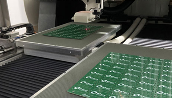
中国を代表するPCBレーザーダパネリングマシンメーカー
ワンストップPCBデパネルソリューション
If you’re still relying on mechanical routers, you’re playing a dangerous game with physical stress and microscopic component cracking. By moving to laser systems, high-end electronics plants are essentially deleting those headaches from the equation. We’re talking zero tool wear, precision down to ±20 microns, and the complete elimination of field failures caused by board flexure.
If you are an Engineering Manager or Quality Director, let’s cut straight to the chase: switching to a PCB laser cutting machine isn’t just a fancy “high-tech” upgrade anymore—it’s a non-negotiable risk mitigation strategy.
If you’re still relying on mechanical routers, you’re playing a dangerous game with physical stress and microscopic component cracking. By moving to laser systems, high-end electronics plants are essentially deleting those headaches from the equation. We’re talking zero tool wear, precision down to ±20 microns, and the complete elimination of field failures caused by board flexure.
As solutions experts who live and breathe factory floor reality—specifically with automotive and medical device giants—we’ve seen the tide turn. The conversation in NPI meetings has shifted from “Can we get away with routing this?” to a top-down mandate: “Standardize laser depaneling across all new lines.”
Before we can appreciate the laser solution, we must look at the real pain points that keep quality managers awake at night. Mechanical separation methods—like routers, V-scoring, and punching—rely on physical contact and brute force. This introduces variables that are incredibly difficult to control in a 24/7 manufacturing environment.
Your day shift runs perfectly. Your Cpk values are solid. But somewhere in the middle of the night, the mechanical router bit wears down just a fraction of a millimeter. By morning, you have fraying on the FR-4 edges, pulled fibers on your flexible printed circuits (FPCs), and a pile of scrap requiring manual inspection. Mechanical bits degrade from the very first cut. As they dull, the friction increases, the localized heat rises, and the mechanical vibration transferred to the board spikes exponentially.
This is the single biggest driver for laser adoption in high-reliability sectors. A perfectly assembled board might pass end-of-line In-Circuit Testing (ICT), only to fail in the field six months later due to thermal cycling. The culprit is almost always mechanical stress.
According to component failure analysis, flex cracking is the most common failure mode for Multilayer Ceramic Capacitors (MLCCs). When a PCB bends during mechanical depaneling, the brittle ceramic body of the MLCC cracks along the termination-to-ceramic interface. Larger case sizes, such as 1206 and 1812, located near the breakaway tabs are incredibly vulnerable to the tension created by a mechanical router.
When a mechanical router chatters through FR4, the stress easily spikes above 800 µstrain. These micro-cracks are invisible to the naked eye and often pass basic electrical testing, only to manifest as leakage currents or complete shorts later. For an automotive airbag sensor or a medical life-support device, this is a catastrophic and unacceptable risk.
Expert Insight: While component manufacturers offer “soft-termination” capacitors to absorb some board flex, these are expensive band-aids. The root-cause engineering solution is to stop bending the board in the first place.
Even if you are currently transitioning your lines, our top layout advice for NPI engineers is to keep large MLCCs at least 3 to 5 mm away from any V-groove or routed edge. If miniaturization demands tighter placement, you cannot rely on mechanical routing. You must route those high-density panels using a non-contact pcb singulation laser system to guarantee zero stress transfer.
From an engineering perspective, switching to a laser system is about engineering absolute certainty into your process. Here is why the industry leaders are standardizing this technology.
Unlike routers that generate heavy shear and bending moments, modern UV lasers utilize “cold ablation.” The high-energy, short-wavelength laser beam breaks the molecular bonds of the substrate without transferring physical force or excessive heat. Because it is a non-contact tool, a laser depaneling machine consistently keeps mechanical stress below 50 µstrain. This is a 95% reduction in stress compared to mechanical methods, completely eliminating the risk of MLCC flex cracking.

High-density interconnect (HDI) boards demand tight tolerances. While mechanical routers are physically limited by the bit size (usually 2.0mm to 3.0mm) and suffer from runout, laser depaneling achieves kerf widths as narrow as 20 µm to 50 µm. Furthermore, advanced laser routing provides superior accuracy, allowing for intricate cuts and complex geometries with tolerances as low as ±20 microns.
Beyond physical dimensions, there is the critical issue of cleanliness. Mechanical routing generates fiberglass dust and copper swarf. Even with industrial vacuums, micro-particles settle on the board. The IPC-5704 standard strictly dictates the cleanliness requirements for unpopulated printed boards, warning that microscopic ionic and particulate contamination can lead to dendritic growth, electrical shorts, and premature product failure.
Because laser cutting vaporizes the material rather than grinding it, the process generates zero milling dust. We consistently see manufacturers achieve pristine, carbonization-free edges that easily pass stringent cleanliness standards without requiring secondary, water-intensive washing processes.
Traditional SMT lines require different mechanical setups for different substrates. A premier laser system seamlessly transitions between materials. With a simple software recipe change, you can cut rigid FR-4, delicate polyimide FPCs, Rigid-Flex combinations, Liquid Crystal Polymer (LCP), and even advanced ceramics.
Before pushing a new substrate into mass production, we always recommend running a small qualification batch to evaluate the Heat-Affected Zone (HAZ). By fine-tuning the UV laser’s pulse energy, frequency, and cutting speed, you can perfectly dial in the recipe. This allows you to completely avoid edge carbonization or burning, even when cutting white solder masks or highly sensitive flexible circuits. Save these optimized parameters into the machine’s library for instant recall.
The transition to laser technology is not anecdotal; it is heavily backed by global manufacturing data. The global market size for laser PCB depaneling machines was valued at approximately USD 350 million in 2023. Driven by the relentless push for electronic miniaturization and high-precision cutting, this market is projected to reach USD 600 million by 2032, exhibiting a compound annual growth rate (CAGR) of 6.2%.
The automotive sector is leading this charge. With the electrification of vehicles, modern EVs contain thousands of complex chips compared to a few hundred in legacy vehicles. Automotive plant managers are explicitly specifying a UV laser cutting machine for new lines because the cost of a single field failure dwarfs the capital expenditure of the equipment.

Let’s look at the financial math of Yield vs. Kerf Width:
By utilizing a narrower kerf, you can pack more individual boards onto a single standard production panel. We have seen clients increase their panel yield by 15% to 30% simply by switching to laser. When you multiply 20% more boards per panel by thousands of panels per month, the material savings alone often pay for the machine.
| Metric | Mechanical Router | UV Laser Depaneling System |
| Mechanical Stress | > 800 µstrain (Varies with tool wear) | < 50 µstrain (Constant, non-contact) |
| Cutting Tolerance | ±100 µm | ±20µm |
| Kerf Width | 2.0 mm – 3.0 mm | 20 µm – 50 µm |
| Edge Quality | Prone to burrs, fibers, requires deburring | Smooth, pristine, dust-free |
| Tool Consumables | High (Bits degrade immediately) | Zero (Non-contact beam) |
| Cleanliness | Fails strict IPC-5704 without washing | Inherently compliant |
Do not treat your laser as an isolated offline process if you are running high-volume manufacturing. For maximum ROI, integrate your PCB depaneling system directly into your SMT line. By utilizing SMEMA protocols and connecting the machine to your Manufacturing Execution System (MES), you ensure 100% traceability. When a Tier-1 medical or automotive client audits your facility, you can pull up the exact cutting parameters, laser power logs, and timestamp data for every single serialized board. This level of control is the ultimate endorsement of your factory’s quality.
On thick FR4 straight cuts, a router might look faster on paper. But when you factor in zero downtime for bit changes, no secondary washing/deburring, and near-zero scrap, laser wins on Total Throughput (OEE). Especially for FPC and thin rigid-flex, laser is the undisputed speed king.
Not with a properly calibrated UV laser. We aren’t using heat-heavy CO2; modern UV systems use “cold” pulses that safely break chemical bonds. The result is a clean, carbon-free edge that passes even the most stringent medical and automotive audits.
Don’t just look at the machine price. Look at the Total Cost of Quality. Calculate your current cost of router bits, the labor for manual inspection/deburring, and the massive liability of a single field failure. Most high-volume manufacturers reach their break-even point within 12 to 18 months just on material savings and yield improvements.
Absolutely. Modern PCB laser depaneling systems are designed for full Industry 4.0 integration. They utilize standard SMEMA protocols to “talk” to your existing conveyors and can be fully integrated with your Manufacturing Execution System (MES). This gives you 100% traceability—you can pull up the exact laser power, cutting speed, and timestamp for every single serialized board. When a Tier-1 auditor asks for proof of process control, you don’t show them a logbook; you show them a digital dashboard.
This is where the laser truly leaves everything else in the dust. A mechanical router bit is basically a ‘dumb’ tool—it just can’t handle the mixed densities of Rigid-Flex or the fragility of ceramics very well. With a laser, though, the ‘tooling’ is all in the software. You just adjust your settings, and the machine pivots from cutting thick FR4 to fragile FPC or Alumina substrates in seconds. You’re trading mechanical downtime for software-driven speed.
If your team can handle a modern SMT mounter, they can handle a laser system. The interface is highly visual and CAD-based. Instead of manually teaching “points” to a router, you import your Gerber files, and the software generates the toolpath automatically. Maintenance is also significantly simpler because there are no moving parts in contact with the board—meaning fewer mechanical breakdowns and no constant calibration of spindle runout.
For factories handling complex, high-reliability electronics, the debate is effectively over. The risk of field failures and the hidden costs of mechanical wear make routers a major liability. Standardizing on high-precision laser technology isn’t just a process tweak; it’s a strategic move for your brand’s reputation.


