
Don't worry, contact Our boss immediately
Don't rush to close it, now, please talk to our boss directly. Usually reply within 1 hour.
China's leading manufacturer of PCB Laser Dapaneling Machine
One-Stop PCB Depaneling Solutions
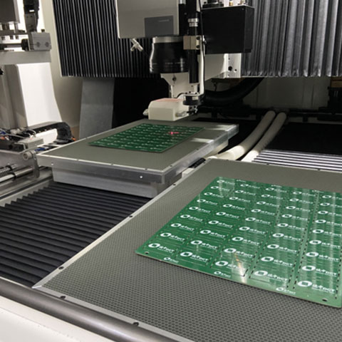
Operator dependency becomes expensive long before it appears on a labor-cost report. In a large PCB factory, one manual touch…
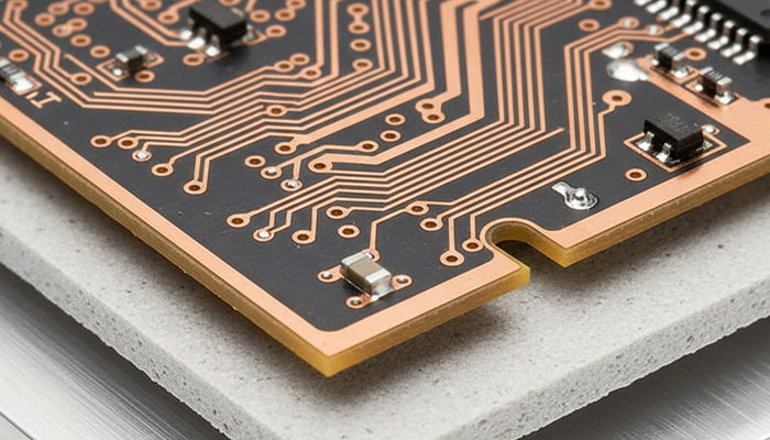
A great machine helps you break terrible old habits. You can finally stop dumping baked boards onto a messy manual table. It hooks right up to your moving belts and it reads barcodes all by itself.
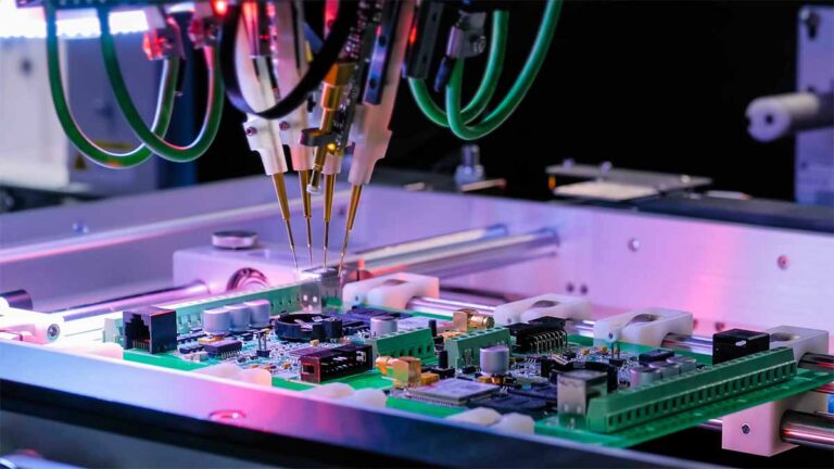
By eliminating the physical bending that cracks ceramic LED chips and MLCCs, you can boost your final yield by up to 5% and virtually eliminate field failures.
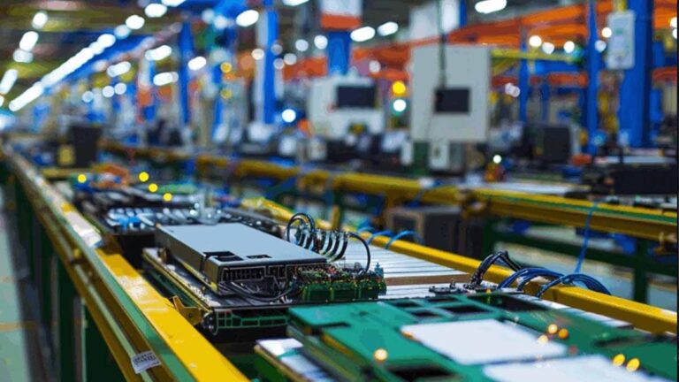
In a high-mix factory, the challenge is not only “how fast can we cut one panel?” The bigger question is: how can we run many board types, materials, batch sizes, and customer requirements without slowing down the whole production system?
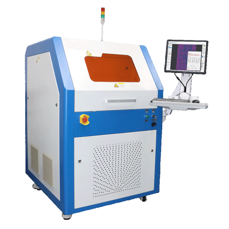
By utilizing a non-contact UV laser process called "cold ablation," we guarantee zero mechanical stress on the board. This completely eliminates edge cracking, protects delicate internal vias, and allows you to safely place components within 0.1mm of the board edge.
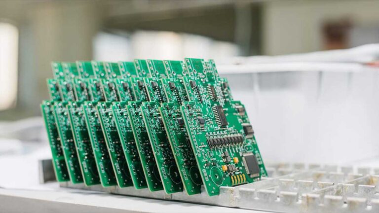
Then, during the absolute final step of separating the panels, a mechanical router bit dulls, vibrates, and causes a microscopic fracture in a $500 medical PCBA.
By standardizing your production lines with a pcb laser cutting machine, you instantly decouple your edge quality from the physical variables of PCB design. The benefits are massive and immediate.
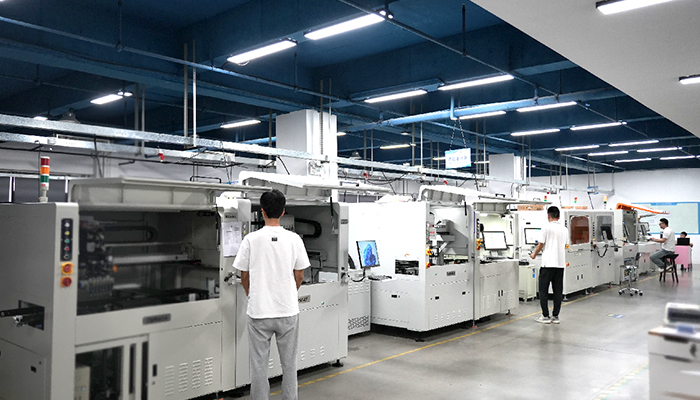
The benefits are massive and immediate: zero upfront tooling costs, zero mechanical stress transferred to delicate surface-mount components, and the unparalleled flexibility to jump from cutting rigid automotive FR4 boards to delicate medical polyimide flex circuits within the same afternoon.