- Ceramics (Al₂O₃/AlN, HTCC/LTCC): Use UV (355 nm) with multi-pass, low fluence; picosecond beats nanosecond for the cleanest edges. Expect ±20–25 µm cut accuracy with minimal chipping when fixturing and extraction are dialed in.
- IMS (metal-core: Al/Cu): Non-contact laser depaneling avoids conductive swarf and stress. UV handles dielectrics; Green (532 nm) improves coupling to copper. Plan for narrow kerf and recipe-driven passes; consider DFM to minimize full-thickness metal removal when possible.
1) Materials at a Glance
Ceramics (Al₂O₃/AlN, HTCC/LTCC): Extremely hard, brittle, thermally conductive, low CTE. Mechanical tools induce cracks and particles; laser ablation is wear-free.
IMS (Insulated Metal Substrates): Copper circuit + dielectric + Al/Cu (sometimes stainless) core. Great for thermal spreading but reflective/heat-sinking—needs tuned laser strategy.
2) Wavelength & Pulse Regime (What Works Best)
Ceramics
- UV 355 nm is the default; ps-UV gives the smallest HAZ and least micro-cracking.
- Use multi-pass cutting with low fluence and higher rep rates; keep velocity constant.
IMS
- Dielectric & soldermask: UV ablates cleanly.
- Copper: 532 nm couples better than IR; UV also works with tuned fluence.
- Metal core: full-depth laser removal is possible but DFM (e.g., local recess, thinner core, partial score) often yields higher takt and less heat load.
3) Edge Quality Playbook (Ceramic & IMS)
- Pass strategy: Many shallow passes > fewer deep passes (reduces chipping/HAZ).
- Optics: Telecentric lens + well-calibrated galvo; verify spot size at focus.
- Extraction: High-efficiency fume/debris removal; lens protection shields.
- Cooling cadence: For thick or high-k stacks, interleave passes or scan segments to limit local heat.
- Verification: Inspect with micrographs; track HAZ width, edge roughness, and any micro-cracks.
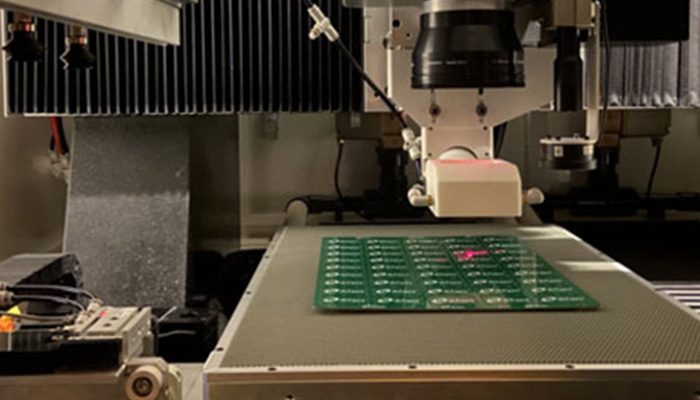
4) Fixturing & Vision
- Vacuum hold-down on granite/bridge platforms; add carriers for thin LTCC/HTCC or small IMS coupons.
- Flatness control: Height sensing if the stack warps under heat load.
- Registration: CCD fiducials or pattern matching; if no targets, use DIL modules.
- Bad-board handling: Mark and skip defective circuits to protect yield.
5) Design-for-Laser (DFL) Rules of Thumb
- Minimum radius: ≤ 0.1–0.2 mm is routine with UV (recipe/model dependent).
- Slot/window width: As low as ~0.2–0.3 mm with tuned passes.
- Keep-out: State your copper/component keep-out; UV enables very tight distances.
- IMS tip: Where possible, avoid long full-thickness core cuts—use notches, thinner cores, or local reliefs to shorten metal path length.
6) Throughput Math (Simple Estimator)
Panel time (rough):
Tpanel ≈ (Total cut length / vector speed)
+ (N_fid × align_time)
+ load/unload + overhead
Laser often wins OEE by eliminating bit changes, tool wear drift, and swarf clean-ups, especially on complex contours.
7) IMS-Specific Pitfalls & Fixes
- Reflectivity & heat sink effect: Use Green/UV, more passes, and steady scan speeds; pre-heat is usually unnecessary if pass strategy is right.
- Conductive debris risk (mechanical): Laser produces no metallic swarf; pair with good extraction to keep edges clean.
- Burr at copper edges: Slight defocus on finishing pass + proper fluence smooths the lip.
8) What “Good” Looks Like (Targets)
- Cut accuracy: ~±20–25 µm
- Repeatability: ~±2–3 µm
- Kerf: ~20–60 µm (material/recipe dependent)
- Ceramic chipping: None visible at low magnification; micro-chipping minimized in micrographs
- IMS edges: Swarf-free, minimal discoloration, no delamination of dielectric
9) Model Picks (by Job Type)
- Small/medium ceramic or IMS coupons: DirectLaser H1 (300×350 mm)
- Offline daily ceramic/IMS panels: DirectLaser S2 (350×350 mm, granite)
- Inline PCBA depaneling: DirectLaser S4 (track-inline, 350×350 mm)
- Inline higher UPH: DirectLaser H3 (dual-platform, 300×300 mm)
- Large/multi-up arrays: DirectLaser H3 330D (350×520 mm)
- Big or complex boards / thick stacks: DirectLaser H5 (520×520 mm; up to 580×580)
10) Sample-Cut Checklist (Send This for Fast Results)
Material + thickness (Al₂O₃/AlN/LTCC/HTCC or IMS core) · Copper stack-up · Dielectric type/thickness · Target kerf/edge limits · Keep-out to copper/components · Panel/board size & array · Takt/UPH · Inline/Offline + MES · CAD (Gerber/ODB++/DXF/Excellon) · Reference photo.
FAQ (Short)
- Will UV/Green damage nearby parts? Proper multi-pass recipes keep HAZ low; it’s non-contact (no mechanical stress).
- Can we cut fully through an aluminum core? Yes, but takt may drop—consider DFL to reduce metal path length or use a hybrid approach (partial relief + finish cut).
- How do we prove quality? Provide micrographs, edge-roughness and HAZ measurements, and—on IMS—resistance/insulation checks across the cut.