Don't worry, contact Our boss immediately
Don't rush to close it, now, please talk to our boss directly. Usually reply within 1 hour.
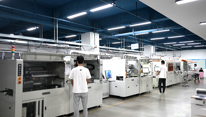
China's leading manufacturer of PCB Laser Dapaneling Machine
One-Stop PCB Depaneling Solutions
The benefits are massive and immediate: zero upfront tooling costs, zero mechanical stress transferred to delicate surface-mount components, and the unparalleled flexibility to jump from cutting rigid automotive FR4 boards to delicate medical polyimide flex circuits within the same afternoon.
As a team of process engineering solutions experts who spend our days walking the floors of high-mix, low-volume (HMLV) contract electronics manufacturers (EMS), we are constantly asked one critical question by plant managers: “How do we protect our Overall Equipment Effectiveness (OEE) when we are forced to change board layouts five to ten times in a single shift?”
Here is the direct, experience-based answer: you must completely eliminate mechanical tooling from your separation process. By standardizing your production lines with a pcb laser cutting machine, you can instantly reduce your production setup times from hours to mere seconds. Because the laser is a 100% software-driven, non-contact tool, there are no custom routing fixtures to mill, no mechanical router bits to replace, and no expensive physical die sets to swap out. You simply load the new digital DXF design file, and the machine adapts instantly.

The benefits are massive and immediate: zero upfront tooling costs, zero mechanical stress transferred to delicate surface-mount components, and the unparalleled flexibility to jump from cutting rigid automotive FR4 boards to delicate medical polyimide flex circuits within the same afternoon.
In this comprehensive guide, we will break down the hidden costs of mechanical setup times, explain the engineering behind laser flexibility, and share our best practices for deploying this technology in a fast-paced contract manufacturing environment.
To understand why lasers are taking over, we first have to look at the severe limitations of traditional mechanical separation methods in an HMLV environment.
In traditional high-volume mass production—such as manufacturing millions of identical smartphone boards—spending three weeks and $3,000 to fabricate a custom die-punch or a dedicated routing jig makes financial sense. The setup cost and time are easily amortized over a massive production run. However, the high-mix model is the exact antithesis of this. In an HMLV scenario, you might run a batch of 500 boards for an aerospace client on Tuesday morning, and immediately switch to a 1,200-board run for an industrial IoT sensor by the afternoon. Every unique PCB design requires a new set of upfront investments in tooling and programming.
The Mechanical Router Bottleneck
Mechanical CNC routers require dedicated, product-specific aluminum jigs to hold the PCB panel securely. This is mandatory to prevent high-frequency vibration chatter from destroying the board during the physical cutting process. Every time a new product runs, your operators must undergo a grueling changeover routine:
This changeover process routinely takes 30 to 45 minutes. If you perform four changeovers a day, you are losing three hours of profitable, machine-running production time. Furthermore, if your client requests a sudden mid-production design change—such as shifting a breakaway tab by just 2mm—your physical routing fixture is instantly rendered useless. You have to halt production and wait days for the machine shop to cut a new one. In an industry where speed to market is a competitive advantage, mechanical bottlenecks are unacceptable.
When we upgrade an EMS client’s facility to a laser depaneling machine, the transformation in operational agility is profound. Here is exactly why you should choose this technology to conquer high-mix challenges:
Laser depaneling replaces physical hardware with digital software. If a client updates a board revision, your CAM engineer simply updates the digital cut path on their computer. Production resumes in five minutes, completely bypassing the machine shop. There is no waiting for custom pins, clamps, or base plates. This fundamentally changes the economic equation of small batch runs, turning a loss-leader project into a highly profitable one.
💡 Best Practice 1: Digitize and Standardize Your Cut FilesStop relying on physical layout templates. Train your CAD and CAM teams to immediately export the mechanical cut path as a standard DXF file the moment a client sends their Gerber data. Modern laser systems feature intuitive CAM software that allows you to drag-and-drop this DXF directly into the machine. You can map out the cutting sequence, assign laser power levels based on material thickness, and save the recipe to the machine’s library in under ten minutes. When the job comes back three months later, loading it takes exactly three clicks.
Contract manufacturers are taking on increasingly dense, miniaturized boards. Mechanical routers create intense shear forces and bending moments. To avoid long-term reliability issues and latent micro-cracking in Multi-Layer Ceramic Capacitors (MLCCs), engineers must aim to keep mechanical stress below 200 microstrain during the cutting process. However, as physical router bits dull—which happens continuously from the very first cut—friction increases, often pushing stress levels well beyond safe limits.
Lasers operate via non-contact ablation. The focused beam vaporizes the substrate without transferring a single ounce of physical bending force to the panel. This guarantees that delicate components located less than a millimeter from the board edge remain 100% safe.
In a high-mix plant, material diversity is a daily challenge. A premier UV laser cutting system allows your morning shift to process standard 1.6mm rigid FR4 panels, and your afternoon shift to switch to incredibly delicate Polyimide flexible printed circuits (FPC), Rigid-Flex assemblies, or even metal-core boards. You do this all without changing a single piece of mechanical hardware—you simply load a different optical recipe.

From a process engineering standpoint, the Return on Investment (ROI) for a laser system in a contract manufacturing environment is heavily driven by the elimination of downtime and the eradication of consumable costs. Let’s look at the hard data comparison:
| Metric | Mechanical CNC Router | Custom Die-Punch | UV Laser Depaneling |
| Tooling Lead Time | 3 to 5 Days (Jig fabrication) | 2 to 4 Weeks | 0 Days (Instant DXF upload) |
| Line Changeover Time | 30 to 45 Minutes | 60+ Minutes | < 2 Minutes (Software load) |
| Tool Wear / Consumables | High (Bits dull continuously) | Medium (Die sharpening) | Zero (Non-contact beam) |
| Cost per Design Change | $500 – $1,500 (New fixture) | $2,000+ | $0 (Digital file edit) |
Beyond setup speed, we have to talk about quality control. When dealing with high-end medical or aerospace clients, bare board cleanliness is paramount. The IPC-5704 standard strictly governs the cleanliness requirements for unpopulated printed circuit boards, establishing quantitative limits to prevent microscopic ionic and particulate contamination.
When a mechanical router grinds through FR4, it creates an abrasive fiberglass and copper dust storm. Even with localized vacuums, particulates settle into the pores of the solder mask, which can later cause dendritic growth and electrical shorts. Because laser depaneling utilizes high-energy photons to vaporize the material into a microscopic gas (which is instantly extracted through a HEPA filter), the process is inherently dust-free. It effortlessly meets IPC-5704 requirements without forcing the manufacturer to invest in secondary, water-intensive board washing stations.
💡 Best Practice 2: Leverage Smart Fiducial RecognitionIn high-mix environments, operator loading errors during rapid changeovers are incredibly common. Instead of relying on tight-tolerance physical pins to hold the board perfectly straight, rely on optical alignment. Ensure your pcb depaneling system utilizes high-resolution downward-looking vision cameras. The machine will automatically scan for the panel’s fiducial marks. If an operator loads the panel slightly skewed, the software mathematically rotates and aligns the laser’s cut path in real-time. This guarantees ±20µm precision without requiring time-consuming mechanical clamping adjustments.
The shift away from mechanical routing in HMLV environments is not just a trend; it is accelerating globally. Market data proves that contract manufacturers are voting with their capital expenditures. The global Automatic PCB Laser Depaneling Machines market size was valued at USD 56.1 million in 2024, and is projected to surge to USD 83.6 million by 2032.
Even more telling is the adoption rate at the factory floor level. Recent market analysis shows that an astonishing 62% of new PCB assembly lines installed in 2024 incorporated laser depaneling systems over mechanical ones, a significant jump from just 48% in 2021.
This surge is heavily driven by the automotive contract manufacturing sector. With modern electric vehicles (EVs) containing massive amounts of complex, high-density PCBs, automotive clients are demanding zero-defect manufacturing. Consequently, laser depaneling adoption in automotive PCB production grew at a massive 28% compound annual growth rate (CAGR) between 2022 and 2024. If you are an EMS provider bidding on modern automotive or EV contracts, having a laser system is rapidly transitioning from a “nice-to-have” to an absolute prerequisite.
💡 Best Practice 3: MES Integration for Zero-Touch ChangeoversTo completely conquer the high-mix setup time problem, you must connect your pcb singulation equipment directly to your factory’s Manufacturing Execution System (MES).
Here is how it works in practice: When a new batch of panels arrives at the laser station via the SMEMA conveyor, the machine’s internal scanner reads the 2D barcode on the panel edge. It queries your central MES server, verifies the work order, and automatically downloads the correct cutting recipe. The laser power, cutting speed, and exact vector path adjust instantly without human intervention. The operator never even touches the screen, reducing line changeover time to absolute zero and entirely eliminating the risk of human error.
When we present laser technology to QA managers transitioning from routing, the most common objection we face is: “Won’t a laser burn the edges of my board, leave carbon dust, or damage nearby traces?”
It is a highly valid concern if you are looking at outdated CO2 lasers (10.6µm wavelength) that rely purely on thermal melting to cut through substrates. However, modern high-end SMT lines solve this by utilizing advanced Ultraviolet (UV) nanosecond or picosecond lasers.
UV lasers operate on the principle of “cold ablation.” Because the UV wavelength (typically 355nm) carries extremely high photon energy, it directly breaks the molecular and chemical bonds of the FR4 resin or polyimide. So, the trick is that it zaps the material away so quickly it doesn’t even get the chance to heat up the fiberglass around it. Once the engineers find that ‘sweet spot’ with the settings, the heat damage is basically zero. You get these incredibly clean cuts without any carbon buildup or rough edges, and the nearby copper doesn’t feel a thing.
In a high-mix, low-volume environment, your margins really come down to one thing: how fast—and how safely—you can pivot from one run to the next.
Let’s be honest, traditional mechanical routing has become a massive bottleneck. Between the custom fixtures, constant bit replacements, and manual Z-axis tweaks, it’s just eating up too much uptime. Modern EMS facilities can’t afford that kind of drag anymore.
By moving to a software-driven laser system, you’re basically removing all that physical friction. You’re protecting your clients’ high-value boards from mechanical stress, and more importantly, you’re turning a stressful 45-minute changeover into a 30-second digital command. It’s about working smarter, not harder.For contract manufacturers looking to protect their OEE and scale their capabilities, it is the ultimate operational upgrade.
A: If you are running very thick, simple, straight-line cuts on standard FR4 panels, a mechanical router might possess a faster linear cut speed. However, in high-mix contract manufacturing, you must calculate Total Throughput. Because the laser requires zero downtime for bit changes, zero time for fixture swapping, and eliminates secondary manual deburring or washing, the total daily throughput of a laser system is consistently higher across diverse product mixes.
A: Generally, no. Most advanced laser systems now use universal flatbeds, adaptable pin-and-honeycomb bases, or specialized vacuum tables. Since the laser is a non-contact tool, it doesn’t exert any physical pushing or pulling force on the board. This means you can skip the expensive, custom-milled aluminum jigs—there’s simply no need to “aggressively” clamp the panel down.
A: If your CAD team has the DXF file ready, a process engineer can import the file into the machine’s CAM software, assign the cutting speed and laser power based on the material, and run the first article test in under 10 minutes. For recurring products already saved in the system’s library, the setup time is just the few seconds it takes to scan a barcode and load the saved recipe.
A: Not at all. Unlike older CO2 lasers that rely on heat, modern UV lasers use “cold ablation” to vaporize the substrate by breaking chemical bonds rather than burning them. When paired with high-capacity industrial fume extraction and HEPA filtration, the process is incredibly clean. It easily meets IPC-5704 bare board cleanliness standards, leaving you with carbonization-free edges and zero fiberglass dust.
A: Absolutely. This is the primary advantage for high-mix contract manufacturers. Through a simple software adjustment to the laser’s frequency, pulse width, and speed, the exact same machine can seamlessly transition from cutting rigid 1.6mm FR4 motherboards to excising incredibly delicate, paper-thin polyimide flex circuits without any mechanical tool changes.


