걱정하지 마세요. 지금 당장 우리 사장님께 연락하세요.
서둘러 닫지 마시고, 지금 바로 저희 사장님께 직접 말씀해 주세요. 보통 1시간 이내에 답변해 드립니다.
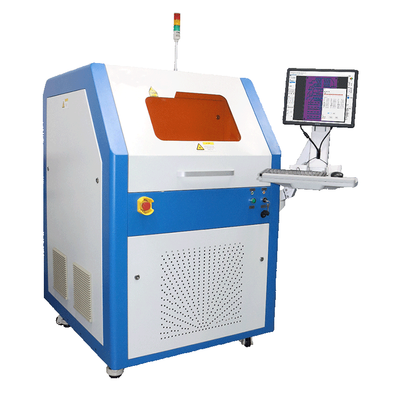
중국 최고의 PCB 레이저 다패널링 기계 제조업체
원스톱 PCB 디패널링 솔루션
By utilizing a non-contact UV laser process called "cold ablation," we guarantee zero mechanical stress on the board. This completely eliminates edge cracking, protects delicate internal vias, and allows you to safely place components within 0.1mm of the board edge.
The Bottom Line Up Front: If your Electronic Manufacturing Services (EMS) facility is experiencing a high volume of edge cracks, fractured MLCCs, or torn microvias on your High-Density Interconnect (HDI) boards, standard mechanical routing is the root cause. As solutions experts who spend our days analyzing production yields on high-end SMT lines, we can tell you plainly: the friction and vibration from physical router bits are destroying your tightly packed components.
The permanent, engineering-backed solution we implement for our clients is upgrading to a pcb laser cutting machine. By utilizing a non-contact UV laser process called “cold ablation,” we guarantee zero mechanical stress on the board. This completely eliminates edge cracking, protects delicate internal vias, and allows you to safely place components within 0.1mm of the board edge. This upgrade secures your production yield and immediately qualifies your factory for high-margin, miniaturized automotive and medical contracts.
We know the frustration you face on the factory floor. Your engineering team spends weeks optimizing an HDI layout. You utilize microvias, tight trace pitches, and via-in-pad technologies to fit maximum functionality into a tiny wearable or automotive sensor. The board prints perfectly, passes Automated Optical Inspection (AOI), and survives the reflow oven without a hitch.
Then, during the absolute final step—separating the finished board from the production panel—a spinning physical router bit vibrates. That mechanical shockwave travels through the substrate, fracturing a $5 ceramic capacitor right near the breakaway tab. You have just lost the expensive components, the bare board, and all your labor hours.
Let’s cut out the fluff. We are going to dive straight into the engineering data to explain exactly why mechanical routing is failing your HDI designs, how laser technology permanently solves it, and how we help factories implement this upgrade.
In standard, low-density FR4 boards, a bit of physical vibration during singulation is usually tolerable. But in the world of High-Density Interconnects, the margin for error shrinks to absolute zero.
When you use a standard mechanical laser routing machine (or a traditional spindle router), a physical 2.0mm or 3.0mm metal bit tears through the FR4, polyimide, or ceramic substrate. This relies on friction. As that router bit dulls—and it begins dulling from the very first cut—it requires more force to push through the material. This introduces severe shear forces and bending moments into the board.
In the electronics manufacturing industry, we measure this physical bending force in “microstrain” (µstrain). Multi-Layer Ceramic Capacitors (MLCCs) are incredibly brittle. Because they cannot bend, any flex in the HDI substrate translates directly into a microscopic fracture within the capacitor’s layers.
Here is the hard data we reference when auditing a factory:
When you are manufacturing complex boards with thousands of microscopic solder joints, you cannot rely on an operator remembering to change a physical router bit before it gets too dull. You need a process that is inherently stress-free.
Expert Best Practice 1: Conduct a Live Strain Gauge AuditIf you are currently experiencing intermittent electrical testing failures on edge-placed components, stop guessing. We strongly recommend renting or buying a strain gauge. Attach the sensor directly next to the routing path of your most dense HDI panel and run your standard mechanical routing program. If your readout spikes over 500 microstrain, your depaneling machine is actively destroying your yield. It is time to pause the line and transition to a non-contact method.
To eliminate edge cracks, we must remove physical friction from the equation entirely. This is why top-tier EMS providers are migrating to a modern uv laser depaneling system.
A common hesitation we hear from SMT project managers is: “Won’t the intense heat from a laser burn my delicate microvias or carbonize the board edges?”
This is a valid concern if you are talking about outdated CO2 lasers. However, HDI processing requires a completely different technology.
Modern systems utilize a short-wavelength Ultraviolet (UV) laser, typically operating at 355nm. Unlike a CO2 laser (which uses an infrared 10.6μm wavelength to thermally melt and burn through material), a UV laser triggers a photochemical reaction.
This process is known in the industry as “cold ablation.” The high-energy UV photons directly break the molecular bonds of the copper, dielectric, and FR4 materials. The material is instantly vaporized layer by layer before the heat has a chance to spread outward into the board.
Because of cold ablation, the Heat-Affected Zone (HAZ) is microscopic. You get a hermetically sealed, perfectly smooth edge with zero carbonization, zero fiberglass dust, and absolutely no thermal degradation to the microvias located right next to the cut line.
We don’t just recommend laser technology based on engineering theory; we recommend it because the market demands it. As consumer electronics and medical devices become smaller, component density per square inch is skyrocketing.
According to deep market intelligence reports, the transition away from mechanical stress is becoming a strict requirement:
Here is a side-by-side technical comparison of why you need to upgrade:
| HDI Processing Metric | Mechanical Router System | UV Laser Depaneling | The Engineering Benefit for You |
| Kerf Width (Waste) | 2.0 mm to 3.0 mm | 20 µm to 50 µm | Maximize panel space. Nest more HDI boards per production sheet. |
| Mechanical Stress | 500 to 1000+ microstrain | < 50 microstrain | 100% elimination of vibration-induced MLCC microcracks. |
| Component Clearance | Minimum 1.0 mm to 2.0 mm | As tight as 0.1 mm | Crucial for ultra-dense wearables, smartphones, and HDI sensors. |
| Edge Quality | Prone to burrs and copper dust | Hermetically sealed edge | Instantly passes strict IPC-A-600 Class 3 visual inspections. |
Expert Best Practice 2: Redesign Your Panels to Leverage the 50-Micron KerfA massive mistake we see factories make is buying a laser and continuing to use their old router panel designs. Mechanical routers force you to leave 2.5mm “mouse bites” or wide routing channels between individual sub-panels. A UV laser only requires a 50-micron kerf. By sitting down with your CAD engineers and tightening your layout to utilize zero-clearance cuts, we routinely help our clients pack 15% to 30% more boards onto a single substrate. The savings in bare board material alone usually pays for the laser machine within the first year.
When upgrading to an inline pcb depaneling system, it is not just about the cut; it is about securing the entire handling process. Manual handling is the enemy of HDI reliability. If an operator manually snaps a V-scored board or forcefully loads a routed panel into a tray, they are introducing the exact bending stress we are trying to eliminate.

HDI boards are thin—often 0.8mm or less—and they contain multiple sequential lamination layers. This makes them highly susceptible to slight warpage during the reflow oven phase. If a rigid mechanical router cuts a warped board, the physical bit will miss the intended path, ruining the edge. Modern laser systems solve this by using high-resolution vision cameras. The system scans the fiducial marks on the fly, dynamically adjusting the galvanometer scanners and the focal height to perfectly match the real-time warpage of the board.
Medical and automotive OEMs now require absolute traceability. Modern laser machines connect via SMEMA protocols directly to your line conveyors. They scan 1D or 2D barcodes, execute the perfect stress-free cut, and send the exact cutting parameters (laser power, speed, timestamp) to your Manufacturing Execution System (MES). If an auditor asks for proof of process control, you don’t show them a paper logbook; you show them the digital dashboard.
Expert Best Practice 3: Stop Milling Custom FixturesMechanical routing requires custom-milled physical jigs and fixtures for every single product variant. This costs money and delays NPI (New Product Introduction). Laser systems use software-defined paths and vacuum-table holding. To run a new HDI board, you simply upload the new DXF or Gerber file. This agility allows your factory to switch from producing a high-mix medical board to an automotive EV sensor in seconds, without any physical tooling changes.
To show you exactly how this impacts your bottom line, let’s look at an implementation we recently oversaw for a Tier-1 EMS provider.
The Challenge: The factory was producing ultra-dense, rigid-flex HDI boards for a medical diagnostic device. The layout featured 0201 passive components and highly sensitive ceramic capacitors located just 0.3mm from the panel edge. Using their existing mechanical routing systems, the spindle vibration was causing a catastrophic 14% defect rate. The cracks were microscopic, passing visual inspection but failing during the final in-circuit electrical stress test.
The Solution: We replaced their mechanical routing stations with a fully automated UV laser depaneling platform.
The Results:
To wrap up, here are the top 5 questions we receive from engineering managers looking to resolve their HDI edge-cracking issues.
Answer: Mechanical routers use physical friction. A spinning metal bit tears through the HDI substrate, creating severe vibration and shear forces that bend the board. Brittle components like MLCCs cannot bend, so they crack. A UV laser is a 100% non-contact tool. It uses concentrated light to vaporize the material at a microscopic level, meaning exactly zero physical bending force (under 50 microstrain) is transferred to the board.
Answer: No. Modern UV lasers operate at a 355nm wavelength, utilizing “cold ablation.” Instead of melting the board like older thermal CO2 lasers, the UV photons break the molecular bonds directly. The material vaporizes so fast that the Heat-Affected Zone (HAZ) is limited to just a few microns, completely protecting delicate microvias and fine traces located near the cut path.
Answer: Because there is zero mechanical stress and the laser kerf width is extremely narrow (20 µm to 50 µm), you can safely design your HDI boards with components placed as close as 0.1mm to the board edge. Standard mechanical routing usually requires 1.0mm to 2.0mm of “safe clearance” to prevent vibration damage.
Answer: Yes, incredibly well. Because the cutting path is completely software-controlled via high-speed galvanometer scanners, the laser can easily cut complex curves, sharp internal corners, and intricate rigid-flex contours that are physically impossible for a round mechanical router bit to navigate.
Answer: It is remarkably simple. Modern laser systems are built for Industry 4.0. They are fully SMEMA compliant, allowing them to plug directly into your existing automated loaders, unloaders, and conveyors. They also feature built-in APIs to connect directly to your factory’s MES for real-time barcode scanning and digital traceability.


