걱정하지 마세요. 지금 당장 우리 사장님께 연락하세요.
서둘러 닫지 마시고, 지금 바로 저희 사장님께 직접 말씀해 주세요. 보통 1시간 이내에 답변해 드립니다.
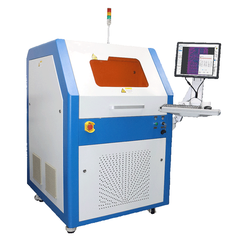
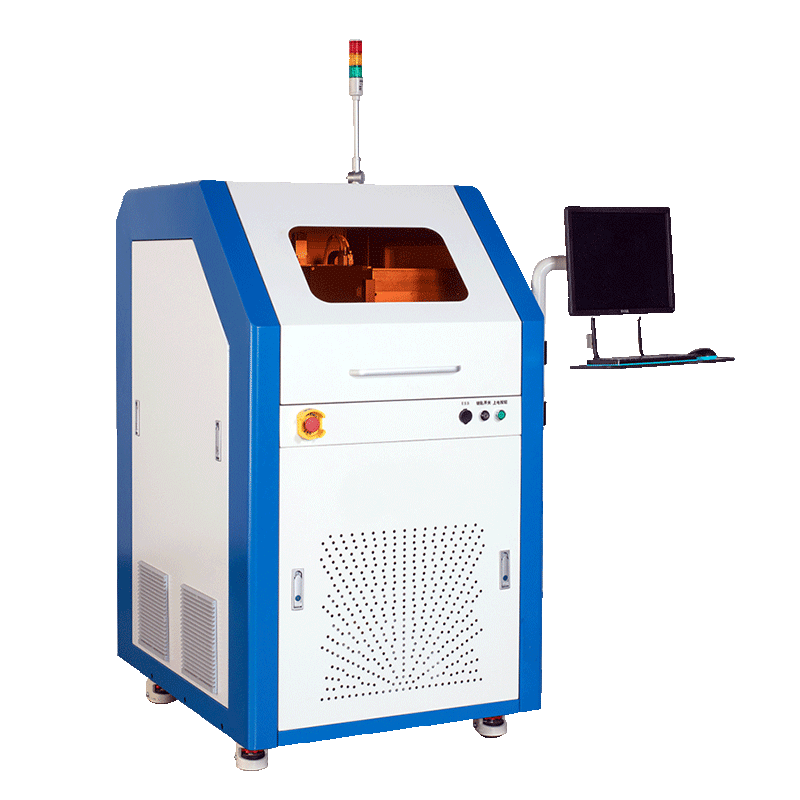
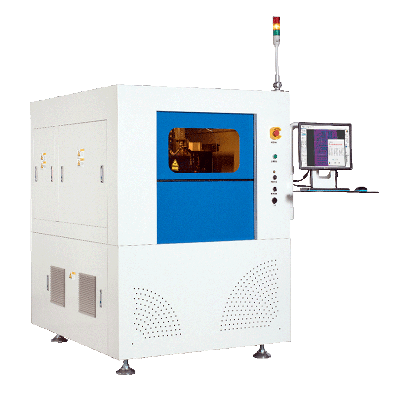
중국 최고의 PCB 레이저 다패널링 기계 제조업체
원스톱 PCB 디패널링 솔루션
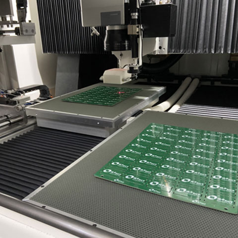
Operator dependency becomes expensive long before it appears on a labor-cost report. In a large PCB factory, one manual touch…

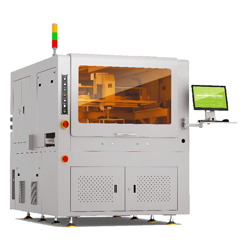
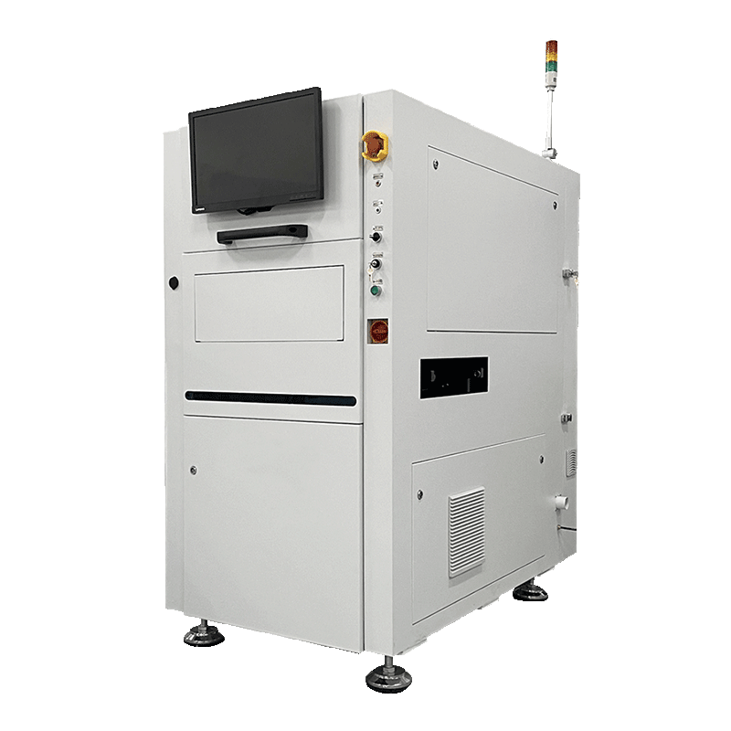
A great machine helps you break terrible old habits. You can finally stop dumping baked boards onto a messy manual table. It hooks right up to your moving belts and it reads barcodes all by itself.
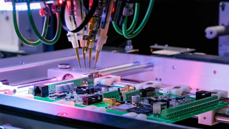
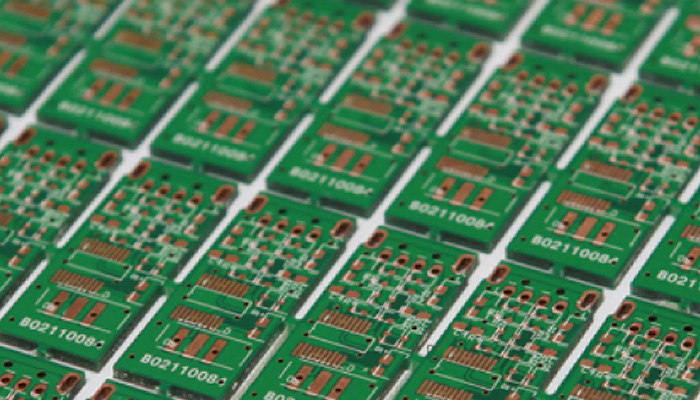
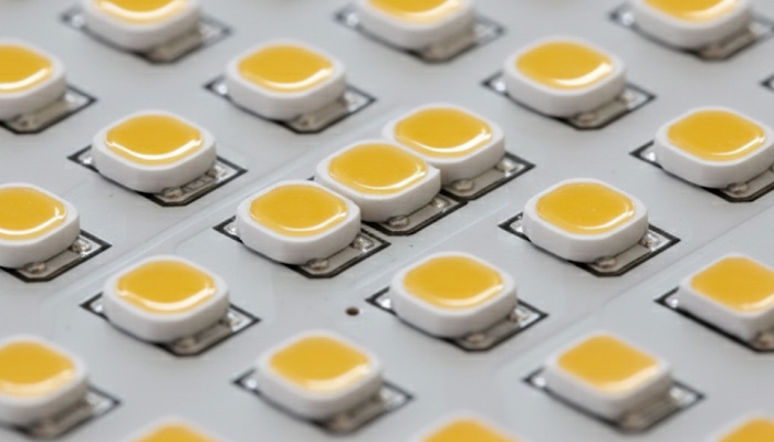
By eliminating the physical bending that cracks ceramic LED chips and MLCCs, you can boost your final yield by up to 5% and virtually eliminate field failures.
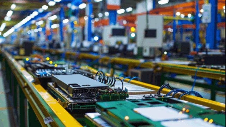
In a high-mix factory, the challenge is not only “how fast can we cut one panel?” The bigger question is: how can we run many board types, materials, batch sizes, and customer requirements without slowing down the whole production system?
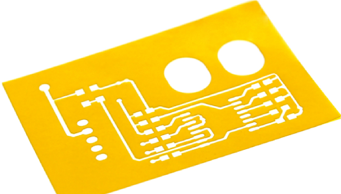
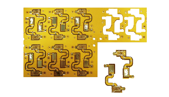
FR-4/FR-5, CEM, FPC/PI, LCP, PTFE/RF, 세라믹(Al₂O₃/AlN), IMS(Al/Cu 코어).
반복성 ±2–3 µm; 절단 정확도 약 ±20–25 µm; 절단 간격은 수십 마이크론입니다.
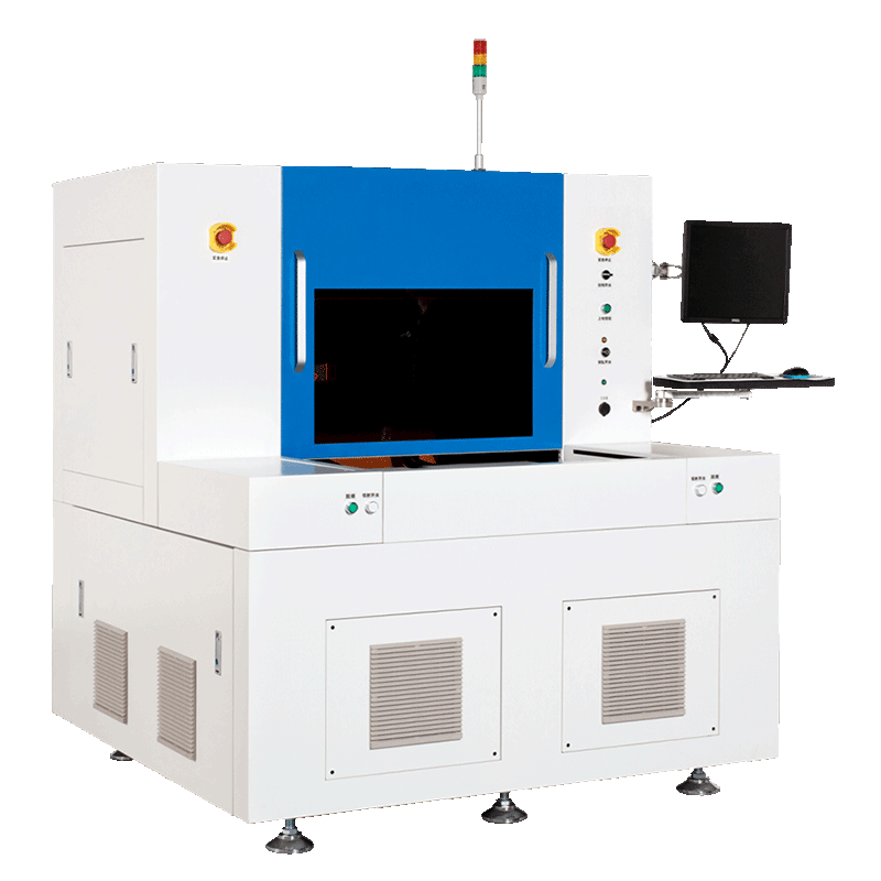
예—S4/H3는 바코드/QR, 레시피 제어, 데이터 로깅을 지원합니다.
UV/Green 공정은 HAZ를 최소화하고, 비접촉 절단으로 기계적 스트레스를 피할 수 있습니다.
거버 RS-274-D/X, DXF, Excellon, Sieb & Meier, HP-GL, ODB++.
네. CAD/패널 세부 정보를 보내주시면 결과와 프로세스 보고서를 보내드리겠습니다.
현장 설치, 운영자 교육, 24시간 원격 지원, 빠른 예비 부품; SLA 옵션.