UV laser depaneling delivers narrow kerf (≈20–50 µm), clean edges, and stress-free separation—raising panel yield and cutting rework versus routing, punching, or milling.
Why UV for PCB Singulation
- Short wavelength (355 nm): high absorption in FR-4, FPC/PI, ceramics → crisp edges, low HAZ.
- Non-contact: no vibration or mechanical stress near components.
- Design freedom: free-form outlines, internal windows/slots, micro-features.
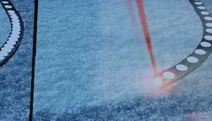
Kerf & Yield: The Math That Pays
- Routing web: ~3.0 mm (bit + margin) → fewer boards per panel.
- UV laser web: ~0.2–0.3 mm (kerf + margin) → +12–30% more boards/panel (typical).
- Result: lower cost/PCB and higher UPH on complex contours.
Edge Quality & HAZ Control
- Multi-pass, low-fluence strategies keep heat input low.
- Telecentric optics + high rep-rate scanning → vertical walls, smooth edges.
- Real-time extraction removes particulates; no conductive swarf.
Practical Design Rules (Quick)
- Keep-out to copper/components: share your target; UV allows very tight keep-outs.
- Tabs/bridges: switch to laser micro-tabs or go tab-less with vision alignment.
- Minimum feature radius: typically ≤0.1–0.2 mm (recipe/model dependent).
- Data: Gerber RS-274-X, ODB++, DXF, Excellon supported.
Material Coverage
- FR-4/FR-5 & HDI — narrow kerf, tight tolerances.
- FPC / rigid-flex (PI/LCP) — burr-free profiles, clean coverlay windows.
- Ceramics (Al₂O₃/AlN, HTCC/LTCC) — chip-free outlines with tuned energy.
- IMS (Al/Cu core) — stress-free, swarf-free depaneling of metal-core boards.
Inline or Offline?
- Inline (track or dual-table): highest takt, MES/traceability, minimal handling.
- Offline (granite base): flexible, cost-effective for high-mix or NPI.
- Both support barcode/QR, bad-board handling, and recipe control.
Quality & Cost Impacts
- Yield↑: no burrs/swarf, fewer edge-defect reworks.
- OEE↑: no bit changes, fewer stoppages, faster changeovers.
- Consumables↓: no routing bits/dies; optics protection and filters are routine.
Quick Specs You Can Expect (Model-Dependent)
- Cut accuracy: ~±20–25 µm
- Repeatability: ~±2–3 µm
- Kerf width: ~20–50 µm
- Typical areas: 300×350, 350×350, 350×520, 520×520 mm (up to 580×580)
Model Picks (by need)
- Compact precision: DirectLaser H1 (300×350 mm)
- Offline daily SMT: DirectLaser S2 (350×350 mm)
- Track-inline PCBA: DirectLaser S4 (350×350 mm)
- Inline dual-table (UPH): DirectLaser H3 (300×300 mm)
- Large dual-table: DirectLaser H3 330D (350×520 mm)
- Large/complex panels: DirectLaser H5 (520×520; up to 580×580)
Sample-Cut Checklist (send this for a fast answer)
Material & thickness · Board/panel size & array · Copper/component keep-out · Edge/HAZ limits · Target takt/UPH · Inline/Offline + MES needs · CAD (Gerber/ODB++/DXF/Excellon) · Reference photo.
FAQ (Short)
- Will heat damage parts? UV recipes keep HAZ low; non-contact avoids mechanical stress.
- How close can we cut to copper? Very close—share your keep-out target; we validate in trials.
- What about ceramics/IMS? Supported with tuned parameters and extraction.
- Can you trace jobs? Yes—barcode/QR, MES, and data logging are available.