TL;DR
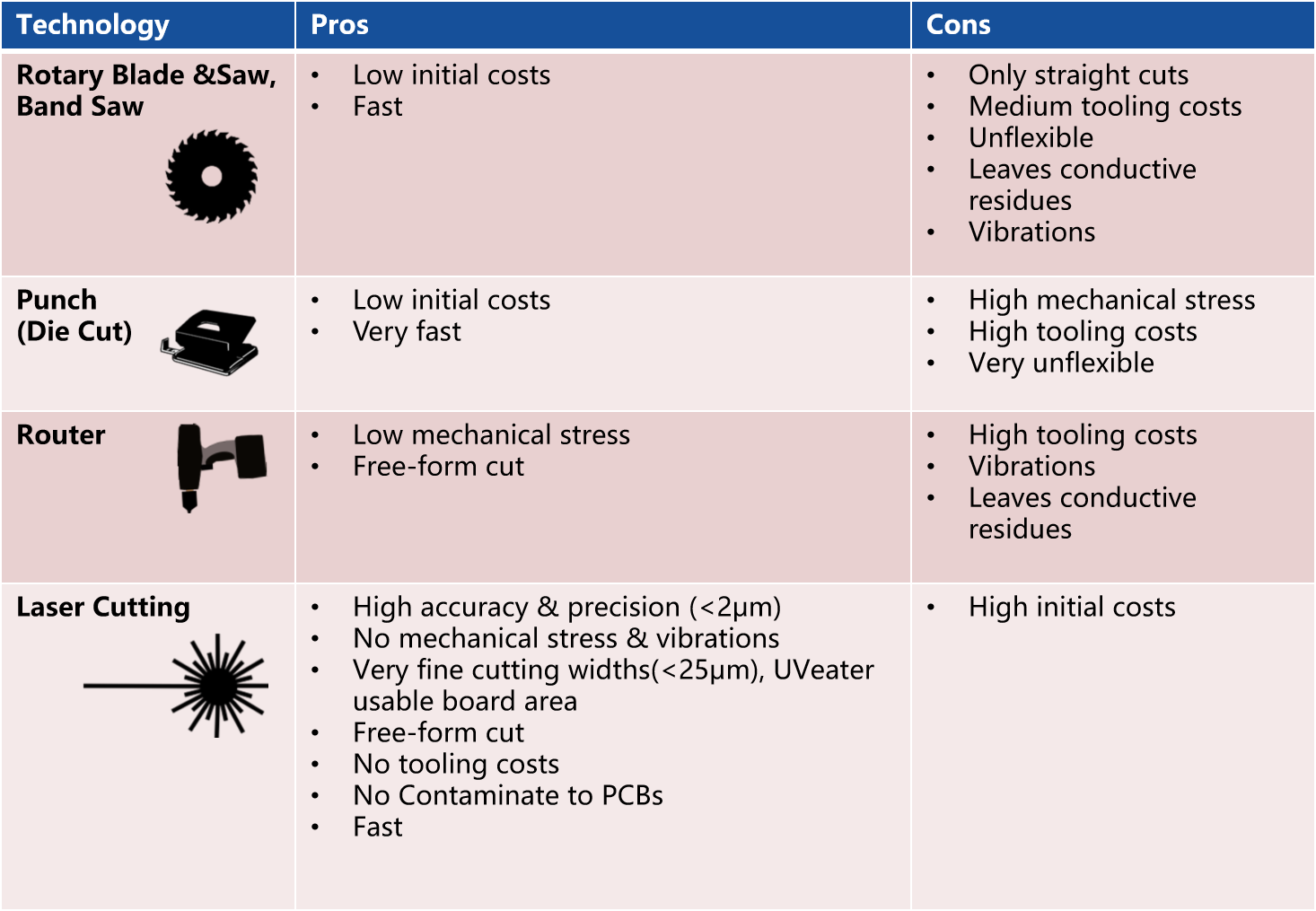
- Laser depaneling (UV/Green) has a narrow kerf (tens of µm) and needs only a small clearance → more boards per panel = higher yield and lower cost per PCB.
- Routing uses a mill/bit (2–3 mm diameter); required web/clearance is much larger → fewer UPH per panel and more scrap area.
- With the same panel, moving from routing to laser cutting PCB board commonly increases panel yield by ~15–30% (example below), while eliminating burrs/swarf and mechanical stress.
1) Kerf & Spacing Basics (the only math that matters)
- Kerf = removal width.
- Routing kerf ≈ bit diameter (e.g., 2–3 mm).
- Laser kerf ≈ 20–50 µm (0.02–0.05 mm), model- and recipe-dependent.
- Required spacing between PCBs (the “web”) must cover kerf plus a safety clearance for tolerance/edge quality.
- Typical routing web: ≈ 3.0 mm (2.0 mm bit + ~1.0 mm margin).
- Typical laser web: ≈ 0.2 mm (0.05 mm kerf + ~0.15 mm margin).
Boards-per-panel (BPP) formula (no nesting/rotations):
UsableWidth = PanelWidth – 2 * RailX
UsableHeight = PanelHeight – 2 * RailY
Across = floor( UsableWidth / (BoardX + SpacingX) )
Down = floor( UsableHeight / (BoardY + SpacingY) )
BPP = Across * Down
2) Worked Example (same panel, different spacing)
Given
- Panel: 250 × 200 mm, edge rails 10 mm each side → Usable 230 × 180 mm
- PCB: 25 × 20 mm
- Case A (Routing): SpacingX = SpacingY = 3.0 mm
- Case B (Laser): SpacingX = SpacingY = 0.2 mm
Compute
- Case A (Routing)
- PitchX = 25 + 3.0 = 28.0 mm → Across = floor(230/28.0) = 8
- PitchY = 20 + 3.0 = 23.0 mm → Down = floor(180/23.0) = 7
- BPP_routing = 8 × 7 = 56
- Case B (Laser)
- PitchX = 25 + 0.2 = 25.2 mm → Across = floor(230/25.2) = 9
- PitchY = 20 + 0.2 = 20.2 mm → Down = floor(180/20.2) = 8
- BPP_laser = 9 × 8 = 72
Yield uplift
Uplift = (72 – 56) / 56 = 28.57%
3) Cost-Per-Board From Panel Price
If the same panel costs $10:
Routing unit cost = $10 / 56 = $0.1786
Laser unit cost = $10 / 72 = $0.1389
Savings per PCB = $0.0397 (~22.2% lower unit cost)
At 500,000 PCBs/year, savings ≈ $19,850/year (excluding quality, rework, and consumables).
4) Sensitivity Snapshot (how spacing moves the needle)
- Routing web 2.5 mm → Across = floor(230/27.5)=8, Down=floor(180/22.5)=8 ⇒ 64/panel
- Laser web 0.3 mm → Across = floor(230/25.3)=9, Down=floor(180/20.3)=8 ⇒ 72/panel
Gain = (72−64)/64 = 12.5%
Even modest web reductions create significant annual savings.
5) Cycle Time & OEE (why “laser depaneling PCB” often wins)
Approximate panel cycle-time:
Tpanel ≈ Lcut / Vcut + Nfid * Talign + Tload/unload + Toverhead
Laser removes:
- Bit-change overhead and tool wear drift
- Clean-up steps from burr/swarf
- Rework from mechanical stress near components
This often offsets similar Lcut/Vcut values, giving higher UPH and OEE—especially on complex contours.
6) Quality Effects That Don’t Fit in One Equation
- Edge quality: no burrs, no conductive swarf; cleaner soldermask edges.
- Near-copper/near-component cuts: low HAZ + micron repeatability → tighter keep-outs.
- Mixed products: parameter/recipe swap in seconds; no dies or routing bits.
- Yield risk: fewer reworks from lifted components, cracked vias, or debris shorts.
7) What We Need to Compute Your Numbers
Send: panel size & rails, PCB size, preferred spacing (or keep-out), target kerf/edge quality, material and thickness, and line mode (offline/inline with or without MES). We’ll return your BPP, unit cost, and a cycle-time estimate.
Model Picks (quick guide)
- Offline: DirectLaser H1 (compact precision), S2 (350×350 mm workhorse)
- Inline: S4 (track-inline 350×350 mm), H3 (inline dual-table 300×300 mm)
- Large / multi-up: H3 330D (350×520 mm), H5 (520×520 mm; up to 580×580)